Development update 11-16-15
So, dear Ehsminer fans, stay tuned for more good news in the upcoming days.
Carl Calder
ACSMA Project Manager

Carl Calder
ACSMA Project Manager
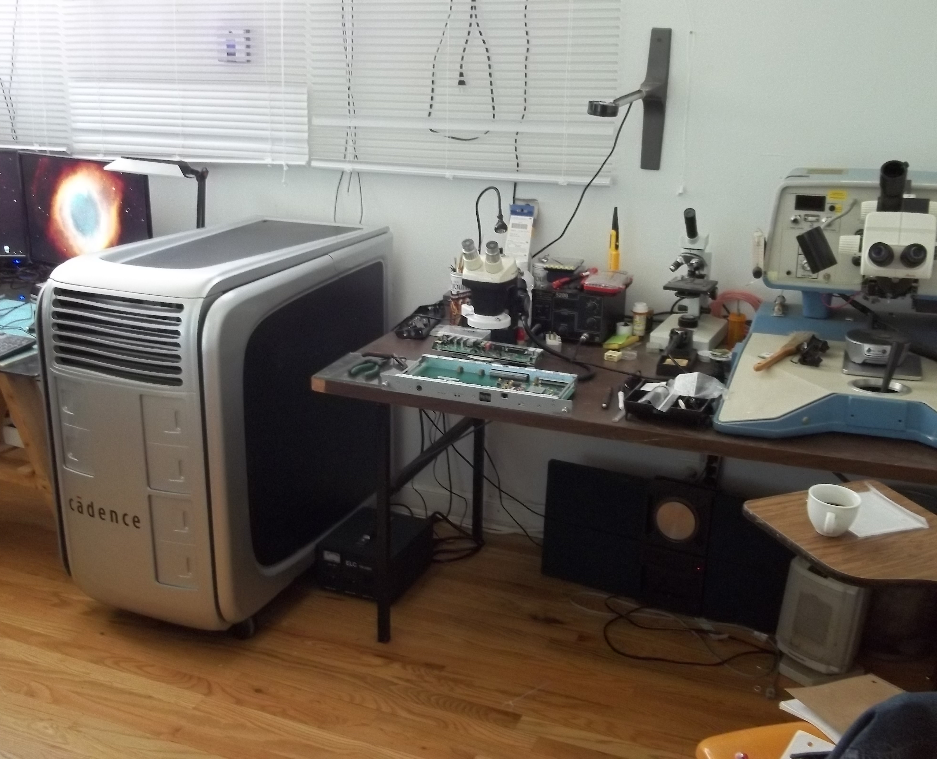
We have been working very hard on the development of ACSMA, our ultra-optimized Scrypt mining architecture. This work is carried out at our ASIC development facility in Denver Colorado USA.
In order to test this very dense logic design several steps have been taken.
Step 1: Test of Reduced Number of Blocs being mined in a simplified version of ACSMA.
This first step required two phases:
1) A simulation of a simplified version of ACSMA is tested thoroughly on a PC server in order to verify the functioning of the complete mining process, configuration and communication.
2) The Logic Synthesis, this is the process of converting high level language used to create ACSMA into hardware primitives like gates memory, FIFOs, registers etc. This is to analyze resources requirement and FPGA verification using an ACHRONIX testbed, for demo purposes.
Step 2: Test of Full version of ACSMA with Reduced Number of Scrypt defined ROMMIX units (this is because of memory requirements).
This second step required two phases:
3) A simulation of mining process is tested on a PC server. Once again this is to verify the full functioning of the mining process of a large scale ACSMA unit.
4) The logic Synthesis and FPGA verification are also used to analyze logic resources using a dual XILINX-ACHRONIX testbed.
This is to showcase our product.
We have been working at all these points concurrently. We can only show now results of point 1 and point 2.
We have our demo of point 3 which is almost ready and will be shown pretty soon.
Once point 4 is finished and exposed, ASIC preparation can start with our ASIC partner.
So we will keep you posted as things are taking shape now.
Best Regards
Ehsminer Team
We are pleased to announce that our communication USB 2.0 high speed interface is fully working now. It was designed to be compatible with the upcoming USB 3.0 new FTDI chip.
This interface will allow a maximum of 480Mb/s delivered to the mining rig in version 2.0. around 8 times more faster in USB 3.0 version.
This is really a huge number even with OS overhead that is more efficient to the achievement of the payload delivery.
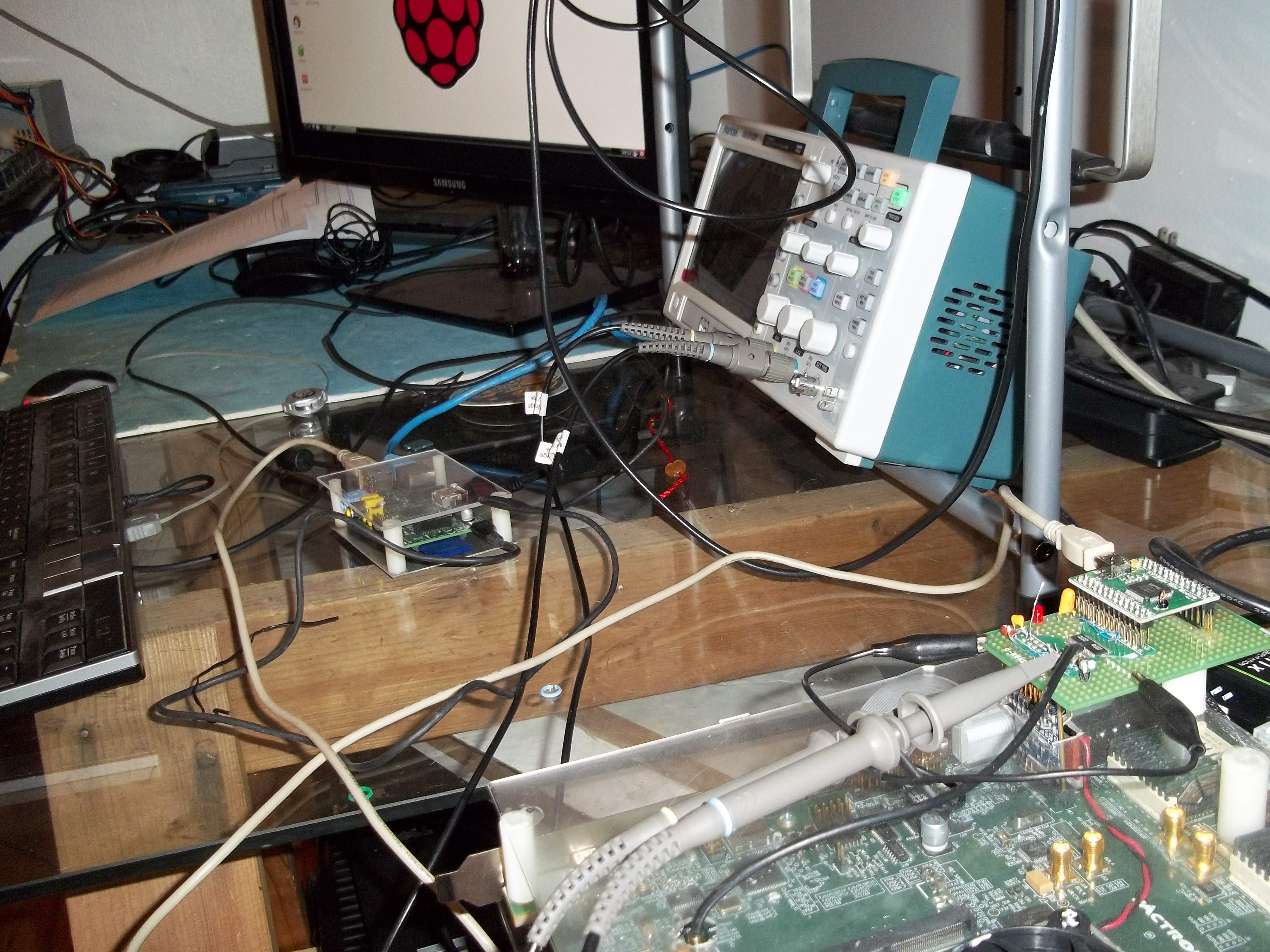
Now we are in the process of putting together the final proof of concept. A Raspberry Pi Linux system will be used as a Host Miner (for the demo only). CPUMiner 0.8 has been adapted to feed ACSMA.
We have gained new knowledge in the Scrypt algorithm and will introduce few changes in ACSMA that will potentially make it a game changer. For reasons of privacy, we can not disclose anything at this point. You need only to male sure that parallel design of the architecture is always going on.
So Merry Christmas and Happy New Year.
Kindest Regards,
Ehsminer Team
This represents a lot of communication bandwidth by using a new host USB 3.0 which is in the making by a supplier FTDI from the UK. It will be probably be available by mid of next year.
We enterprise to design an interface that will be compatible with that new part which is also compatible with the signal level we needed in our Asic chips.
For now, we have to use level shifters and this is proves to be awkward to deal with these configurations of 200 chips or more.
Finally, we are in the process of testing the new level adapters and we hope to have this section working soon.
Kindest Regards,
Ehsminer Team
We are aware that a lot of people are waiting for our proof of work design. Although the functional verification in simulation was done long time ago, we have incurred in several delays in the FPGA port.
Last week we discovered that we were experiencing a lot of noise in the communication interface. This came from the fact that this interface is high speed and it is supposed to support in excess of 200 asic chips. But the real problem was in the Achronix verification platform. Their development tools had a bug and we were confronted with only one option to synchronize the external high speed clock of the communication interface with the communication module inside the FPGA. This created so much noise, so we started to get a corrupted data. It was only yesterday that it was made clear that our communication interface has been properly designed and we can now continue our tests of the ACSMA architecture .
Best Regards,
Ehsminer Team
The ACSMA architecture has become very complex and it has been quite a challenge to devise an efficient testing mechanism. Therefore, we decided to speed up the design validation to read the results of different modules as computation progresses throughout the unit. Then, we compared them to the pure RTL simulation.
For this reason, we modified the communication interface in order to transfer big data streams to upload them to a host computer .This implies a communication test interface that uses most of the USB bandwidth.
At this stage we suffered a set back last week when the signal quality of the main communication clock source was incompatible with the test platform. We tried different approaches as suggested by Achronix support. Although this product is new; there were several inconsistencies that made us take other approaches, as our main goal is not a FPGA port of the ACSMA, but a validation of the design to be ported to an ASIC solution.
We want to clarify an important aspect. As we explained in our last post “Development update 10-17-14” that the hash rate number can be only a power of two.
So, all customers who fully paid their orders of the Wolf V1 512 - 628Mh/s and the 1 - 1.22Gh/s version before this day, will have their orders converted respectively toward the offer of 1024 Mh/s and the 2048 Mh/s version for free.
So please bear with us, as we are laying the foundation for a highly optimized technological solutions for cryptocurrencies.
Best regards,
Ehsminer Team
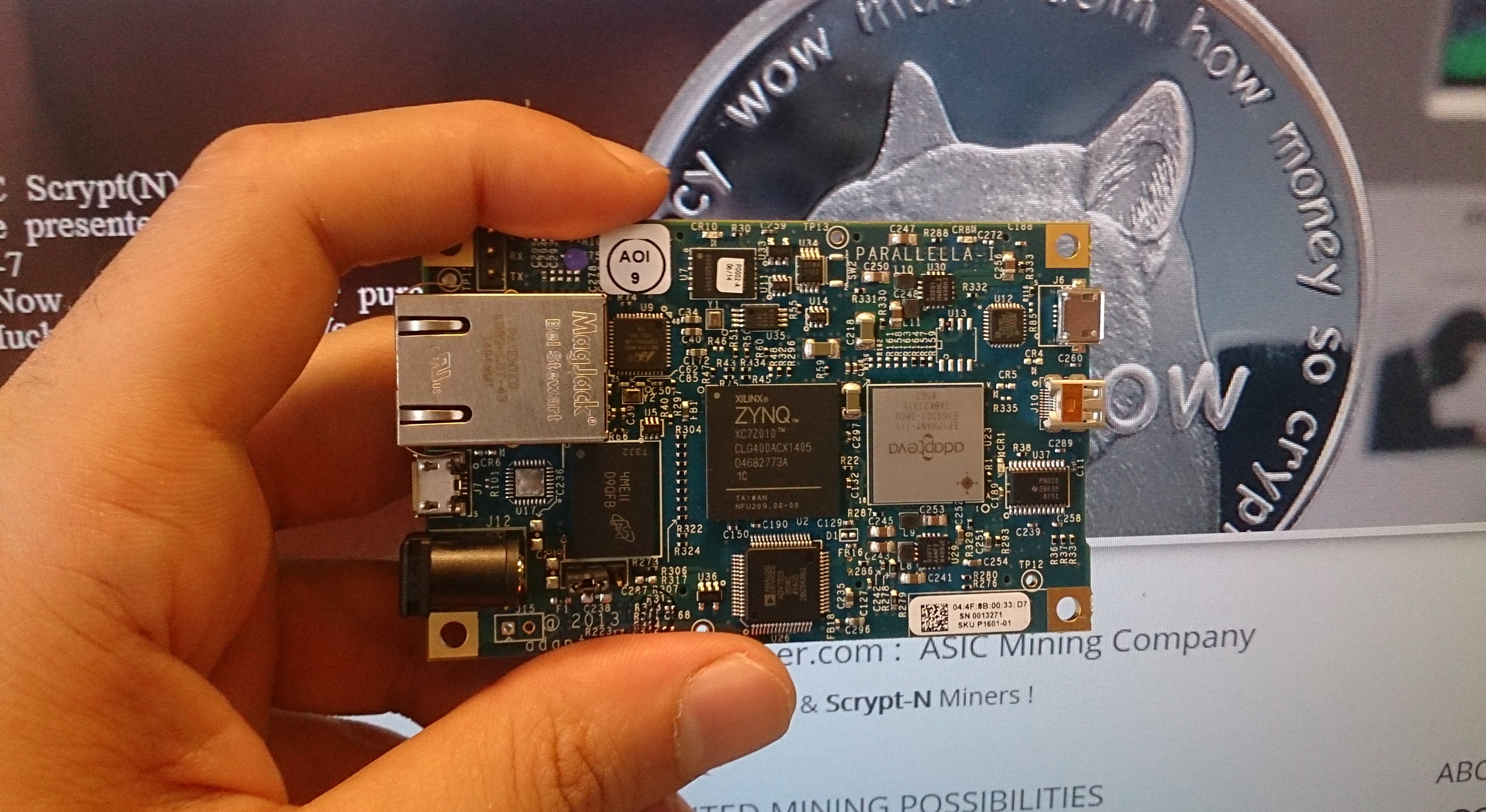
The development of an ASIC is a dynamic process. It requires compromises of price, power, heat and silicon area. This decision is taken while evaluating and testing of the design in the FPGA prototyping phase.
We had only to do a minor change in one of the modules of ACSMA, and this requires to minimize the amount of blocks of RAM we were using, since Nfactor algorithms in ACSMA require memory sizes that must be a power of 2. However, in our ACSMA architecture , Litecoin can use some other sizes.
While the memory reduction was only 5%, it led us to modify several things and then simulate the behavior with a true cycle simulation tool.
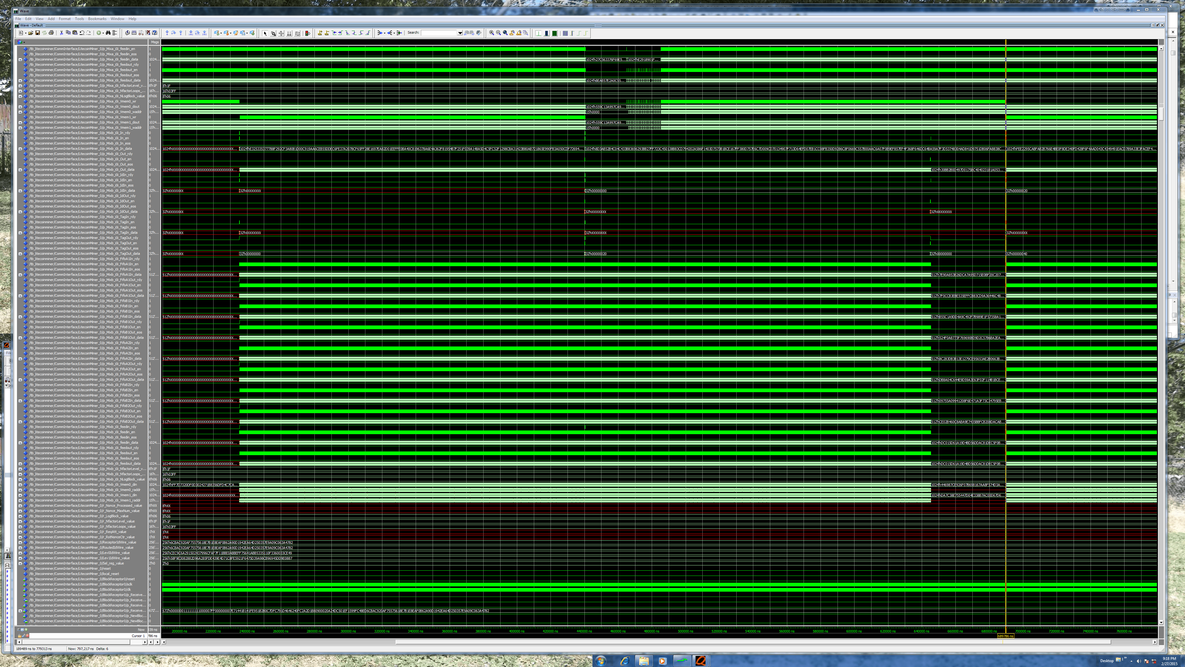
We are now in the process of routing the design and starting to test it in the FPGA evaluation platform by adjusting it to new changes. A new logic analyzer module has been added to follow the Hashing computation in real time.
This design in a simplified form approaches now 4 millions equivalent gates and 200K lines of hardware description language code.
It is important to produce a highly optimized architecture, as this will lessen heat production and power consumption which are considered as key elements of the design.
Kindest Regards
Ehsminer Team
Dear Miners, we wanted to give you a quick update on the progress of work. Be assertive, everything is running well. Here is the advancement of work:
The pieces work by themselves and now the whole system is going to be integrated as a whole unit for proof of concept.
Kindest Regards
Ehsminer Team
The Scrypt algorithm was designed to make its implementation in computer systems very poor.
Although, it is better to optimize it in the FPGA systems, it will not be economically feasible via FPGA to obtain high hashing rates. The only viable solution is an ASIC.
We studied the architecture of the algorithm in order to design a very efficient system that works in a typical brute force of a sheer number of mining cores in other mining solutions. To explain the basics it is better to give some figures:
It is well established that one simple hash on a dedicated digital circuit takes around 150,000 clock cycles to execute. We can infer that the shorter time those cycles take, the higher the hashing rate will be. In other words, the circuit hashing rate can be characterized by FC/150k when FC is the clock frequency of such a circuit.
There are only two possible options to increase the hash rate:
Either, increase the hashing rate of the mining solution by increasing the frequency of the circuit, or using a higher number of cores in parallel.
Solution 1:
Increasing the frequency is a part of our purpose. We are considering the 45nm and 22nm technologies. Besides the price factor, we must also consider the thermal issue.Solution 2:
Mining solution with 2000 to 2500 cores is very high, also it has been considered by other companies.
The number of cores is also another limiting factor.
We chose to look at the architectural side of the multiple mining cores solutions. We realized that, in all cores and at a particular time, only a small fraction of the electronics was being used. Although it is much easier to do silicon copy and paste it on thousands of cores and produce an ASIC very quickly.
This approach is nowhere near optimized, as all of these units cores are not interconnected, neither do they help each other in any way. So billions of expensive transistors are not fully utilized!
This analysis was the basis guideline for the design of ACSMA. To start giving some numbers on the power of ASCMA, we could go back to the original formula for the hashing rate fc/150k.
If we have the possibility to integrate a huge number of hashing cores, let us say 150k cores, the hashing rate of one circuit will be equal to FC.
For a 1 GHz circuit frequency we could obtain 1GHash/S, but this is obviously not possible with the current state of technology. We will need more in excess 50 ASIC chips each with 2500 mining cores with the standard solution.
The architecture of ACSMA addresses the optimization of electronics usage. If the circuit contains 1 billion transistors and all of them are used at the same time ; this optimization is directed to decrease the silicon size of the ACSMA and die ; hence allowing for more equivalent units to increase the size of the embedded high speed rams.
Early in the design of the Litecoin miner we discovered that Nfactor mining was easily possible to add it with few changes. As a matter of fact, ACSMA could also process Bitcoin. This is one of the reasons for the name “Configurable” in ACSMA.
ACSMA has been designed to increase the Hash rate by using an architecture organization. The aim was to produce a HASH per clock cycle. This is not far fetched as it seems. Let’s take the example of the 150k cores architecture. We could run that circuit and produce each 150k cycles a total of 150KHashes (as they are parallel). This is equivalent to 1 Hash per cycle but there is one side effect.
There is a latency of 150kcycles associated, we looked into this and tried to minimize that latency. Although ACSMA cannot escape the curse of the SCRYPT algorithm memory requirements by optimizing the silicon die area to include more memory - it is now possible. ACSMA chips will contain between 2 Gigabits and 4 Gigabits.
ACSMA chips have specialized modules that deal with the memory blocks .The computational power of ACSMA is dependent of the total internal memory given by:
Nu = number of memory units (a minimum of 50 in each chip)
M = Contiguous 1 Megabits memory blocks = 64
Nram = Nu*M: 3.2 Gigabits of total memory
The final value of Nram will be defined in the next design phase, but a minimum of 3.2 Gigabits is part of the design requirements with the ASIC contractor.
Now, our Scrypt implementation can write each 62 Megabits block in 64K cycles. This defines the Hashing power of ACSMA and it means that one unit inside ACSMA is able to produce an equivalent HASH a little over than 1000 cycles. The total hashing capability needs to be multiplied by Nu the number of memory units.
Fc = 600 MHz
The formula for determining the hashing power for Litecoin N = 10 - With basic values :
Hlcpwr = Nu*(fc/1000) (or 30 Mh/s with basic requirements).
With this setting, 1GH mining rig will require 30 chips or so. Our current API addressing scheme will allow using 256 chips.
Nfactor mining is based on huge memory requirements depending on the value of N
Because memory inside an ASIC is a fixed resource, all we can do is use more memory for each hash.
This will reduce mining hash rate of ACSMA Hnfac depending on the value of N, and it can be stated in terms of Hlcpwr as follows:
Hnfac= Hlcpwr/[2^(Nfac-10)]
Which basically means by using the same memory amount inside ACSMA chips, hashing power is halved every time Nfac is increased ?
Now these numbers are just used as requirements for our basic design .The frequency can be increased, and with the reduction of silicon area with which ACSMA was designed in mind, we will increase the memory blocks and therefore the total hashing power.
We love crypto
Ehsminer Team
We are still perfectly on track to release the FPGA prototype in less than 25 days from now. It is quite a monumental task to set up a powerful miner which is fast and reliable. We have already passed the biggest hurdles and we are well on our way to complete the final tasks within our set time frame.
Bellow are the details of our development :
We studied several approaches in order to develop a powerful and configurable architecture that is capable of mining different new SCRYPT oriented toward crypotcurrencies.
The development started by structuring the architecture in high level language which is called HLS conversion to obtain RTL code. We obtained, for purposes of FPGA prototyping, 200K lines of RTL code that were tested in Functional Analysis. This phase was tested with a real cycle simulator.
After Functional simulation, we have now an idea about the resources required to prototype on the FPGA platform. The Scrypt algorithm requires a lot of memory. In a few words the trick is “the faster you can run the algorithm ; the faster you will produce data ; the more memories you will require”.
So, as stated earlier, in order to test an architecture like ACSMA, we needed a FPGA system with a lot of embedded blocks of memory. In our case 80Mbits were the minimum required and only the Achronix FPGA was fast enough and had that big memory.
The next processing phases are physically porting all the RTL code into FPGA logic and memories.
After logic synthesis we started to see our developing architecture in terms of logic primitives.
The Mapping phase is a phase where all is optimized and connected. Now we have converted all language code into FPGA resources and we need only to verify that the conversion process is right and the behavior is equivalent to the functional code we started with.
After Synthesis and mapping is done. The last and more time consuming phase starts:
This phase is iterative as it is very computationally intensive, and demands are very limited to the human intervention.
Only directives are given at the start of the process of routing to guide the routing algorithm.
After this phase, everything becomes easy - we’ll just do the FPGA/ASIC conversion. The FPGA based design can be converted into an ASIC.
First of all, thank you for your patience. We appreciate it since, it has been a while that we updated you with our news.
Most importantly, we are glad to inform you that we are in our final stage of development. We are nearly reaching the testing phase. So, once our hardware is tested, our dear miners will have a large chance for preorder.
We love crypto
Ehsminer Team